

duribility:10,000 cycles
Rated Current:20A-120A
Temperature Rise:30K maximum.
BTB connecting distance:H±0.50mm(customizable)
As the trend towards the miniaturization of electronic devices continues unabated, interconnection solutions between circuit boards face unprecedented spatial challenges. YFS Technology (SZ) Co., Ltd. introduces the MicroBridge series of ultra-high density board-to-board connectors, specifically engineered to meet the demand for high-performance connections within the most stringent space constraints. This product represents our latest breakthrough in miniaturized connection technology, providing the perfect interconnect solution for wearable devices, portable medical instruments, IoT modules, and ultra-thin consumer electronics. MicroBridge is not merely a breakthrough in size, but a leap forward in achieving reliable signal and power integrity within a microscopic footprint. It addresses the fundamental challenge faced by design engineers today: how to pack more functionality into ever-shrinking devices without sacrificing the robustness and performance of each internal connection.

The MicroBridge series distinguishes itself through a set of features engineered for the microscopic scale:
Extreme Miniaturization: The cornerstone of the MicroBridge design is its ultra-fine pitch and exceptionally low profile. It achieves connectivity in spaces previously considered unusable, enabling new industrial design possibilities and more compact product architectures.
Reliability at Micro-Scale: Building a reliable connection at this scale is a significant engineering feat. MicroBridge utilizes advanced materials and a precision dual-beam contact design to ensure stable electrical performance and mechanical retention, resisting the stresses of assembly and daily use in compact devices.
High-Speed Signal Capability: Despite its tiny size, the MicroBridge does not compromise on performance. Its architecture is optimized to support high-speed data transmission, minimizing crosstalk and insertion loss to ensure data integrity in applications like miniature cameras, high-density sensors, and compact communication modules.
Manufacturing Precision & Yield: Designed for high-volume manufacturability, the MicroBridge series features construction and tolerances suitable for automated, precision pick-and-place assembly. This design-for-manufacturing approach ensures consistent quality and high production yields, which is critical for cost-sensitive, high-volume consumer applications.
Implementing the YFS MicroBridge connector delivers key strategic advantages for product development:
Unlocks Radical Miniaturization: It directly enables the next generation of smaller, sleeker, and more portable electronic devices by solving the board-to-board connection bottleneck in tightly packed layouts.
Improves Product Performance-to-Size Ratio: By allowing more components and functions to be integrated into a smaller volume, MicroBridge helps create devices that are not just smaller, but also more powerful and feature-rich compared to their predecessors.
Enhances Design Aesthetics and Ergonomics: The space saved on internal connections can be allocated to larger batteries, more sophisticated sensors, or simply a more appealing and ergonomic external form factor for the end-user.
Reduces Total Interconnection Cost: In many designs, a single MicroBridge connector can replace multiple larger connectors or complex flex cable assemblies, simplifying the Bill of Materials (BOM) and reducing overall interconnection costs.
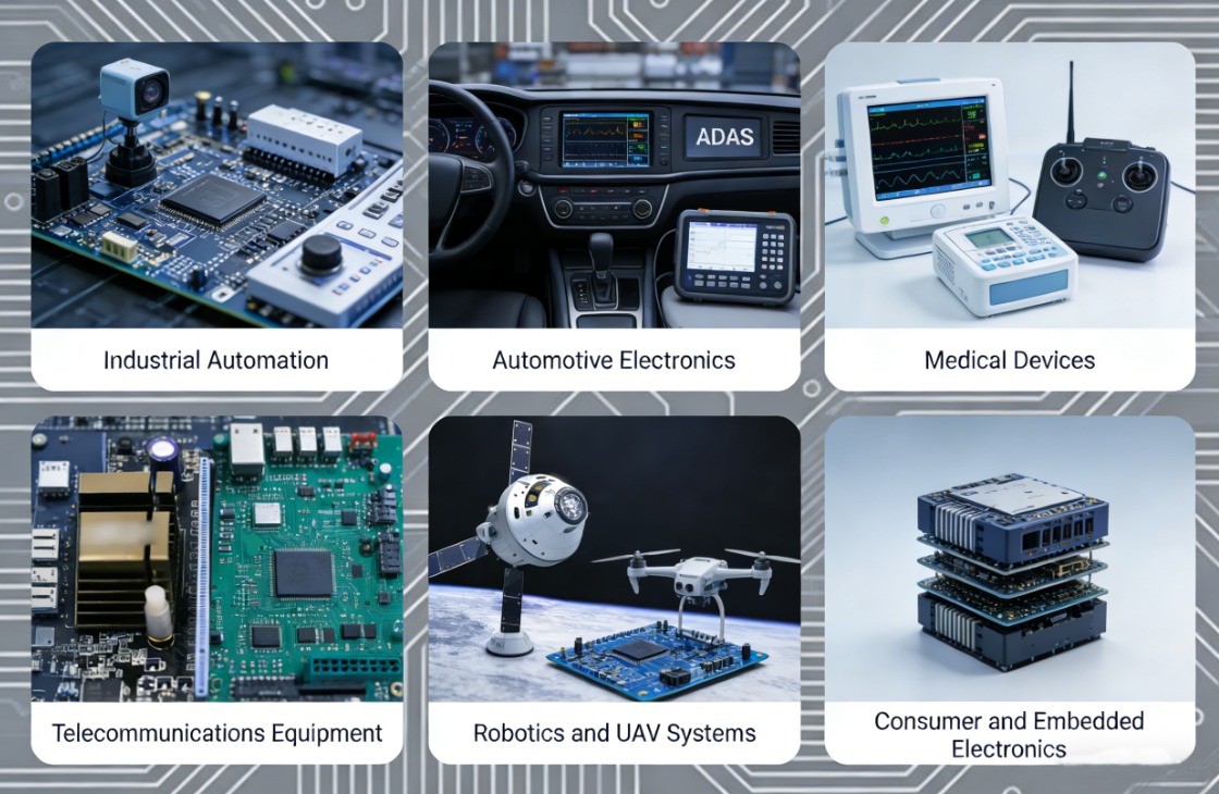
The MicroBridge connector is the enabling technology for a new class of compact electronics:
Wearable Technology: Ideal for smartwatches, fitness trackers, hearables (wireless earbuds), and AR/VR glasses, where internal space is at an absolute premium.
Portable Medical & Diagnostic Devices: Provides critical, reliable interconnections in compact continuous glucose monitors, digital pill cameras, handheld ultrasound probes, and other point-of-care diagnostic tools.
IoT & Edge Sensor Modules: Enables robust connectivity in miniaturized environmental sensors, asset trackers, and smart home modules that require long-term reliability in a tiny package.
Advanced Consumer Electronics: Essential for achieving the sleek profiles of modern smartphones, folding displays, ultra-thin laptops, and compact drone cameras.
Miniature Industrial & Robotic Systems: Used in miniaturized inspection cameras, endoscopic tools, micro-drones, and compact robotic joints where size and weight are critical performance factors.
Q: How does the MicroBridge maintain reliability with such a small size?
A: Reliability is engineered through material science and mechanical design. We use high-performance, durable plastics for the housing and a precision-formed dual-beam contact system. This design provides redundant contact points and sufficient normal force to ensure a stable connection, even under vibration, while our plating process ensures long-term conductivity and corrosion resistance.
Q: What are the biggest challenges in assembling with such fine-pitch connectors?
A: The primary challenges are PCB pad design accuracy, solder paste application, and component placement precision. We provide extremely detailed recommended land patterns and stencil designs. Success requires a well-controlled Surface Mount Technology (SMT) process with good equipment calibration. Our application notes offer comprehensive guidance for assembly best practices.
Q: Can the MicroBridge series handle power delivery in addition to signals?
A: Yes. While optimized for signal density, the series includes configurations with dedicated power contacts. These contacts are designed with a larger cross-section to safely carry the required current for applications like compact modules that need both data and power between boards.
Q: Is there a trade-off between the miniaturization of MicroBridge and its mating cycle life?
A: There is a designed balance. The MicroBridge is rated for a mating cycle life appropriate for its application space (e.g., devices that are not intended for frequent disassembly). For applications requiring higher durability, we recommend alternative series within our portfolio, such as the NexLink, which are designed for more frequent mating/unmating.
Q: What support is available for prototyping with MicroBridge connectors?
A: We strongly recommend using our provided PCB footprint files and 3D models during the design phase. Evaluation samples are available to verify fit and function. For first-time designs, consulting with our applications engineering team during the layout phase can help avoid common pitfalls and ensure a successful integration.
Address:Shenzhen City, China
Mobile Phone:+86 17656553585
Email:davykou0@gmail.com


© 2025 YFS Technology (SZ)Co., Ltd All rights reserved.
This website uses cookies to ensure you get the best experience on our website.


 Phone
Phone